(Junction Field Effect Transistors)
Although there are lots of confusing names for field effect transistors (FETs) there are basically two main types. The reverse biased PN junction types; the JFET or Junction FET, (these are also called the JUGFET or Junction Unipolar Gate FET), and the insulated gate FET devices (IGFET). All FETs can be called UNIPOLAR devices because the charge carriers that carry the current through the device are all of the same type i.e. either holes or electrons, but not both. This distinguishes FETs from the bipolar devices in which both holes and electrons are responsible for current flow in any one device.
The JFET
This was the earliest FET device available. It is a voltage-controlled device in which current flows from the SOURCE terminal (equivalent to the emitter in a bipolar transistor) to the DRAIN (equivalent to the collector). A VOLTAGE applied between the source terminal and a GATE terminal (equivalent to the base) is used to control the source - drain current. The main difference between a JFET and a bipolar transistor is that in a JFET no gate current flows, the current through the device is controlled by an electric field, hence "Field effect transistor". The JFET construction and circuit symbols are shown in fig 3.1.15.
Fig 3.1.15a JFET Construction
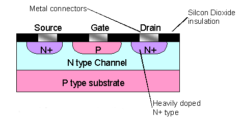
Fig 3.1.15b JFET Circuit symbols
Fig 3.1.15a shows the cross section of a junction FET (JFET) The load current flows through the device from source to drain along a channel made of N type silicon. Hence the majority charge carriers are electrons.
P channel JFETs are also available and the principle of operation is the same as the N channel type described here; but polarities of the voltages that are of course reversed and the charge carriers are holes.
0 komentar:
Post a Comment